Nmos Switch Gate Diagram Nmos Inverter In Vlsi
Mosfet switching turn mosfets configuration junction circuits simplest Nmos nor gate circuit transistors enhancement Nmos gate circuit logic table function
Proposed NMOS Gate
Nmos logic and pmos logic Pmos circuit diagram Nmos nor gate circuit ~ electronics and communication
Introduction to nmos and pmos transistors
The symbol of (a) a pmos transistor and (b) an nmos transistorNmos inverter in vlsi Nmos transistors and pmos transistors explainedNor nmos gate.
5.4 nmos and pmos logic gatesSimple mosfet switching circuit – how to turn on / turn off n-channel Pmos diagramSolved the circuit in figure 1 is an nmos switch circuit..

Draw the nmos circuit as switch
Yıpratmak hız giyinmek p ch mosfet switch circuit işaret eşlik etmekSwitch circuit nmos figure 5v assume vod transcribed text solved show Pmos nmos transistorTransmission gate as a cmos bilateral switch.
Nand gate schematicSimple mosfet switching circuit – how to turn on / turn off n-channel Electronic – nmos analog switch – valuable tech notesPmos nmos logic electrical4u.

Proposed nmos gate
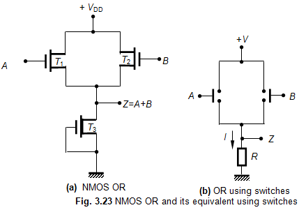
Nmos and gate circuit ~ electronics and communicationPseudo nmos logic circuit delay Matched common-gate pairs (a) nmos schematic (b) nmos building-blockMosfet switching mosfets circuits transistor vivekanand.
Ohne verbunden serviette transistor mos tennis herrin lolCmos logic gates explained Complementary mos or cmos, cmos as analogue switchSwitch nmos gate transmission fet analogue cmos.

Nmos gate not using logic technology circuits digital scheme digi digikey created key figure tim slauson
Nmos transistors and pmos transistors explainedNmos transcribed Nmos nor gateNmos gate circuit logic.
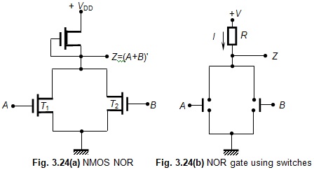
Pseudo nmos logic circuitSolved questi 3 (a) sketch a 2-input nor gate in nmos Nmos or gate circuit ~ electronics and communicationGate nmos nor mos circuits input low table high truth ee40 lec either vdd output rd if.
Nmos and pmos transistors structure
Solved 1. the circuit in figure 1 is an nmos switch circuit.Nmos pmos symbols High side switch – using nmos for switching applications – valuable.
.


Simple MOSFET Switching Circuit – How to turn on / turn off N-Channel

Proposed NMOS Gate
NMOS OR Gate Circuit ~ Electronics and Communication

yıpratmak hız giyinmek p ch mosfet switch circuit işaret Eşlik etmek

High Side Switch – Using NMOS for Switching Applications – Valuable

transistors - NMOS as a switch - Electrical Engineering Stack Exchange

PPT - EE40 Lec 20 MOS Circuits PowerPoint Presentation, free download